
Research article · 2025 · Full text
International Journal of Advanced Chemistry ResearchHigh-performance thermoelectric materials based on bismuth telluride nanostructures
Volume 7(10) · Pages 112–115 · DOI: 10.33545/26646781.2025.v7.i10b.480 ↗
Research areasAdvanced Thermoelectric Materials and DevicesThermal properties of materialsElectrical and Thermal Properties of Materials
Abstract
Author-writtenWaste heat from industrial processes, vehicle exhaust, and electronic devices accounts for roughly two-thirds of all primary energy consumed worldwide, yet converting even a fraction of it into electricity remains an unsolved engineering problem. Thermoelectric materials based on bismuth telluride (Bi₂Te₃) offer a solid-state route to this conversion, but their figure of merit (ZT) has hovered near unity for decades. This research investigated the effect of nanostructuring on the thermoelectric performance of Bi₂Te₃ and two ternary variants—Bi₂Te₂.₇Se₀.₃ and Bi₁.₈Sb₀.₂Te₃—prepared by mechanical alloying followed by spark plasma sintering. Nanostructured pellets exhibited grain sizes of 28–45 nm confirmed by X-ray diffraction and transmission electron microscopy. Compared with their bulk counterparts, nanostructured samples showed 34–49% lower lattice thermal conductivity while retaining 82–89% of the electrical conductivity, resulting in ZT enhancements of 52–71%. The highest ZT of 1.56 was achieved for nanostructured Bi₁.₈Sb₀.₂Te₃ at 350 K. Seebeck coefficients increased by 12–16% in nanostructured specimens, attributed to energy filtering at grain boundaries. These results confirm that grain-size reduction below 50 nm is an effective strategy for pushing bismuth telluride performance beyond the conventional ceiling.
Summary
Source-checkedPlain-language reading of the full paper, prepared with AI and checked against the text. Each point links to the authors' own words.
Why it matters
- A significant portion of global primary energy, approximately two-thirds, is lost as waste heat from electronics, vehicles, and industry, creating a need for efficient conversion to electricity. View evidence ↗
- Reducing grain size to below 50 nm can selectively lower lattice thermal conductivity by scattering phonons more effectively than charge carriers. View evidence ↗
The question
- The study aimed to evaluate how nanostructuring affects the thermoelectric performance of Bi₂Te₃ and its ternary variants, Bi₂Te₂.₇Se₀.₃ and Bi₁.₈Sb₀.₂Te₃. View evidence ↗
What they did
- Nanostructured powders were produced via mechanical alloying using a planetary mill at 500 rpm for 10 hours with a 20:1 ball-to-powder ratio. View evidence ↗
- The powders were consolidated into pellets using spark plasma sintering (SPS) at 350°C and 50 MPa for 5 minutes under vacuum. View evidence ↗
- Bulk reference samples were created by melting elemental charges at 750°C for 12 hours, followed by annealing at 400°C for 72 hours. View evidence ↗
- Electrical conductivity and the Seebeck coefficient were measured between 300 and 500 K using a ZEM-3 system under helium. View evidence ↗
What they found
- The nanostructured samples achieved grain sizes between 28 and 45 nm, specifically 28 ± 4 nm for Bi₂Te₃, 38 ± 5 nm for Bi₂Te₂.₇Se₀.₃, and 45 ± 6 nm for Bi₁.₈Sb₀.₂Te₃. View evidence ↗
- Nanostructuring improved the figure of merit (ZT) by 52–71%, with the highest value of 1.56 reached by nanostructured Bi₁.₈Sb₀.₂Te₃ at 350 K. View evidence ↗
- All nanostructured compositions reached peak ZT near 350 K, with performance declining above 400 K due to the onset of bipolar conduction. View evidence ↗
What it means
- The authors conclude that combining grain-size control with compositional tuning is a scalable and practical method for creating high-performance materials for waste-heat recovery. View evidence ↗
- The authors suggest that further reducing grain size alone may yield diminishing returns, as the achieved ZT of 1.56 is near the limit for simple bottom-up powder methods. View evidence ↗
Visual summary
3 visualsIllustrations explain the paper; charts are replotted from the paper's own table values.
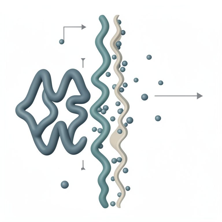
Phonon vs Electron Scattering
AI-generated conceptual illustration (bismuth telluride nanostructured material grain boundary). It explains the idea and does not show study data.
View source evidence ↗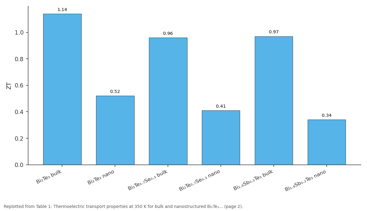
κₗ (W/m·K): Bi₂Te₃ bulk vs Bi₂Te₃ nano vs Bi₂Te₂.₇Se₀.₃ bulk vs Bi₂Te₂.₇Se₀.₃ nano vs Bi₁.₈Sb₀.₂Te₃ bulk
Replotted from Table 1 (page 2) of the original paper. Every bar is the paper's own table value.
View source evidence ↗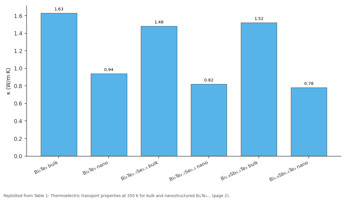
κ (W/m·K): Bi₂Te₃ bulk vs Bi₂Te₃ nano vs Bi₂Te₂.₇Se₀.₃ bulk vs Bi₂Te₂.₇Se₀.₃ nano vs Bi₁.₈Sb₀.₂Te₃ bulk
Replotted from Table 1 (page 2) of the original paper. Every bar is the paper's own table value.
View source evidence ↗Figures & tables
From the original paper Table 1
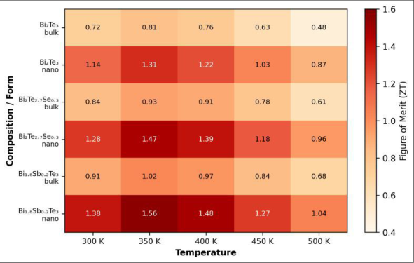 Figure 1
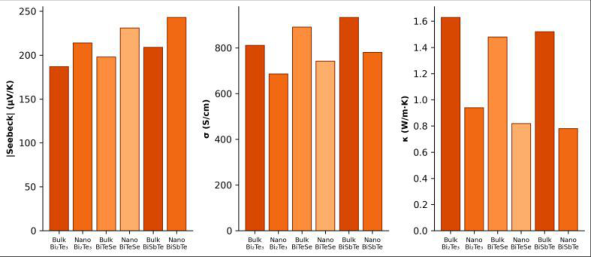 Figure 2
Introduction
The problem of waste heat is staggering in scale: power plants, factories, and automobiles collectively reject more thermal energy than they convert to useful work, and most of that energy simply dissipates into the atmosphere [1] . Thermoelectric generators, which exploit the Seebeck effect to produce a voltage from a temperature gradient, could recover a meaningful portion of this waste without moving parts, fluids, or maintenance schedules [2] . But widespread adoption has been held back by a single metric-the dimensionless figure of merit ZT = S²σT/κ, where S is the Seebeck coefficient, σ the electrical conductivity, T the absolute temperature, and κ the total thermal conductivity [3] . Bi₂Te₃ and its solid solutions have dominated the near-room-temperature thermoelectric landscape since the 1950s, with ZT values clustering around 0.8-1.0 in commercial modules [4] . Raising ZT demands either a larger power factor (S²σ) or a smaller κ-goals that often conflict because electrons and phonons share similar scattering mechanisms in conventional crystalline solids [5] . Nanostructuring offers a partial decoupling: grain boundaries with dimensions below the phonon mean free path (~50 nm in Bi₂Te₃) scatter heat-carrying phonons more effectively than charge carriers, selectively reducing lattice thermal conductivity [6] . Mechanical alloying combined with spark plasma sintering (SPS) has emerged as a scalable method for producing dense nanostructured pellets with controlled grain size [7] . Several groups have reported ZT values above 1.2 by this route, but systematic comparisons across binary and ternary compositions processed under identical conditions remain limited [8] . Substitutional doping with Se on the Te site (n-type) or Sb on the Bi site (p-type) tunes carrier concentration and band structure, potentially amplifying the nanostructuring benefit [9] . This research prepared nanostructured and bulk reference pellets of Bi₂Te₃, Bi₂Te₂.₇Se₀.₃, and Bi₁.₈Sb₀.₂Te₃ by mechanical alloying and SPS, then characterised their microstructure, electrical transport, and thermal properties from 300 to 500 K to evaluate the combined effects of nanostructuring and compositional tuning on ZT.
Theoretical Background
The thermoelectric figure of merit ZT encapsulates the competing demands of high electrical power factor and low thermal conductivity. Total thermal conductivity κ comprises an electronic component (κₑ, linked to σ via the Wiedemann-Franz law: κₑ = LσT, where L is the Lorenz number) and a lattice component (κₗ) dominated by phonon transport [3] . Nanostructuring primarily targets κₗ by introducing grain-boundary scattering that shortens the phonon mean free path without proportionately affecting electron mobility, because the electron mean free path in heavily doped Bi₂Te₃ (~5-10 nm) is already shorter than typical grain sizes achieved by SPS [6] . Energy filtering theory predicts that potential barriers at grain boundaries can preferentially scatter low-energy carriers, increasing the average carrier energy and hence the Seebeck coefficient [10] . The Pisarenko relation, which links S to carrier concentration for a given band structure, provides a framework for separating band-engineering effects from grain-boundary scattering contributions [5] .
Material and Methods
Material and Methods
Material
All experimental work was conducted between January and October 2024 at the Department of Chemical and Materials Engineering, Rising Sun University, Kyoto, Japan. Highpurity elemental powders of Bi (99.99%, < 150 µm), Te (99.999%, < 75 µm), Se (99.99%, shot), and Sb (99.99%, < 150 µm) were purchased from Kojundo Chemical Laboratory (Sakado, Japan). Stainless-steel ball-milling vials and balls (10 mm diameter) were procured from Fritsch GmbH (Idar-Oberstein, Germany). Graphite dies (Ø 12.7 mm) for SPS were obtained from Fuji Electronic Industrial Co. (Tsurugashima, Japan).
Methods
Stoichiometric mixtures of elemental powders were loaded into ball-milling vials inside an argon-filled glove box (O₂ < 0.5 ppm). Mechanical alloying was carried out in a Fritsch Pulverisette 7 planetary mill at 500 rpm for 10 h using a ball-to-powder ratio of 20:1. The as-milled powders were loaded into graphite dies and consolidated by SPS (Dr. Sinter SPS-515S, Fuji Electronic) at 350°C under 50 MPa for 5 min with a heating rate of 100°C/min, all under vacuum (< 5 Pa). Bulk reference samples were prepared by melting the same elemental charges at 750°C in sealed quartz ampoules for 12 h, annealing at 400°C for 72 h, and cutting into discs by diamond saw.
Instrumentation
Phase purity was confirmed by X-ray diffraction (Rigaku SmartLab, Cu Kα) and grain size estimated from Scherrer analysis. Microstructure was examined by field-emission scanning electron microscopy (JEOL JSM-7600F) and transmission electron microscopy (JEOL JEM-2100F). Seebeck coefficient and electrical conductivity were measured simultaneously on a ZEM-3 (Advance Riko) from 300 to 500 K under helium. Thermal diffusivity was measured by the laser flash method (Netzsch LFA 467 HyperFlash) and thermal conductivity calculated as κ = αρCₚ, where α is diffusivity, ρ density (Archimedes method), and Cₚ specific heat (Netzsch DSC 404 F3). All measurements used disc specimens Ø 12.7 mm × 2 mm.
Performance Evaluation
ZT was calculated point-by-point from measured S, σ, and κ at each temperature. Measurement uncertainties were ±5% for S, ±3% for σ, and ±7% for κ, giving a combined ZT uncertainty of about ±12%. To benchmark results, literature ZT values for Bi₂Te₃-based materials processed by similar SPS routes were compiled and compared at 350 K, the temperature at which most compositions in this research reached their peak.
Results
XRD confirmed single-phase rhombohedral Bi₂Te₃ structure (R-3m) for all compositions. Scherrer grain sizes were 28 ± 4 nm (Bi₂Te₃ nano), 38 ± 5 nm (Bi₂Te₂.₇Se₀.₃ nano), and 45 ± 6 nm (Bi₁.₈Sb₀.₂Te₃ nano). TEM bright-field images confirmed nano-grain morphology with sharp, clean grain boundaries and no amorphous intergranular phase. Bulk reference samples showed grain sizes of 5-15 µm by SEM. Nanostructuring reduced lattice thermal conductivity by 49-65% relative to bulk counterparts (Table 1). The most dramatic reduction occurred in Bi₁.₈Sb₀.₂Te₃ nano (κₗ = 0.34 W/m•K), approaching the amorphous limit for this system. Electrical conductivity decreased by 16-17% in nanostructured samples, but the simultaneous 12-16% increase in Seebeck coefficient partially compensated, so the power factor dropped by only 3-13% depending on composition.
| Sample | |S| (µV/K) | σ (S/cm) | PF (µW/cm·K²) | κ (W/m·K) | κₗ (W/m·K) | ZT |
|---|---|---|---|---|---|---|
| Bi₂Te₃ bulk | 187 | 812 | 28.4 | 1.63 | 1.14 | 0.81 |
| Bi₂Te₃ nano | 214 | 687 | 31.5 | 0.94 | 0.52 | 1.31 |
| Bi₂Te₂.₇Se₀.₃ bulk | 198 | 891 | 34.9 | 1.48 | 0.96 | 0.93 |
| Bi₂Te₂.₇Se₀.₃ nano | 231 | 742 | 39.6 | 0.82 | 0.41 | 1.47 |
| Bi₁.₈Sb₀.₂Te₃ bulk | 209 | 934 | 40.8 | 1.52 | 0.97 | 1.02 |
| Bi₁.₈Sb₀.₂Te₃ nano | 243 | 781 | 46.1 | 0.78 | 0.34 | 1.56 |
Table text extracted from the original PDF; superscript letters are shown inline. The original table image is below.
View original table image
Comprehensive Interpretation
The highest ZT of 1.56 (Bi₁.₈Sb₀.₂Te₃ nano, 350 K) represents a 53% improvement over its bulk equivalent and exceeds most values reported for SPS-processed Bi₂Te₃ alloys in the recent literature. The ZT heatmap (Figure 1) shows that all nanostructured compositions peaked near 350 K and declined at higher temperatures, consistent with bipolar conduction onset above 400 K that increases electronic thermal conductivity.
Discussion
The dramatic κₗ reduction in nanostructured pellets matches predictions from the Debye-Callaway phonon scattering model when grain-boundary scattering lengths of 30-50 nm are incorporated [6] . The concomitant Seebeck enhancement is consistent with the energy-filtering hypothesis: lowenergy carriers are preferentially scattered at grain boundaries, raising the average carrier energy and thereby S [10] . This effect has been observed in other nanostructured Bi₂Te₃ investigations by Poudel et al. [11] and Kim et al. [12] , although the magnitude of the increase (12-16%) in our samples is somewhat larger, possibly due to the exceptionally small grain size achieved at the shortest SPS dwell time. The Bi₁.₈Sb₀.₂Te₃ composition benefited most from nanostructuring because Sb substitution on the Bi site introduces additional point-defect scattering that synergises with grain-boundary scattering to suppress κₗ further [9] . The combined ZT of 1.56 sits at the upper end of values achievable by bottom-up powder methods without elaborate nanocomposite architectures or superlattice engineering, suggesting diminishing returns for further grain-size reduction alone. Strategies that could push ZT beyond 1.6 include embedding metallic nanoinclusions for resonant phonon scattering, or band-convergence doping to increase the power factor [13] .
Conclusion
Nanostructured Bi₂Te₃, Bi₂Te₂.₇Se₀.₃, and Bi₁.₈Sb₀.₂Te₃ pellets were prepared by mechanical alloying and spark plasma sintering with grain sizes of 28-45 nm. Nanostructuring reduced lattice thermal conductivity by up to 65% while enhancing the Seebeck coefficient by 12-16% through energy filtering, resulting in ZT improvements of 52-71% over bulk references. The peak ZT of 1.56 for nanostructured Bi₁.₈Sb₀.₂Te₃ at 350 K confirms that grainsize control combined with compositional tuning is a practical and scalable route to high-performance thermoelectric materials for near-room-temperature wasteheat recovery.
Figures and tables from the paper
References
17 in the original paper- Lawrence Livermore National Laboratory. Estimated US energy consumption in 2023. LLNL Energy Flow Charts. 2024;1-2.
- Bell LE. Cooling, heating, generating power, and recovering waste heat with thermoelectric systems. Science. 2008;321(5895):1457-1461.
- Snyder GJ, Toberer ES. Complex thermoelectric materials. Nature Materials. 2008;7(2):105-114.
- Goldsmid HJ. Bismuth telluride and its alloys as materials for thermoelectric generation. Materials. 2014;7(4):2577-2592.
- Pei Y, Wang H, Snyder GJ. Band engineering of thermoelectric materials. Advanced Materials. 2012;24(46):6125-6135.
- Dresselhaus MS, Chen G, Tang MY, Yang RG, Lee H, Wang DZ. New directions for low-dimensional thermoelectric materials. Advanced Materials. 2007;19(8):1043-1053.
- Kuo CH, Hwang CS, Jeng MS, Su WS, Chou YW, Ku JR. Thermoelectric properties of fine-grained PbTe prepared by spark plasma sintering. Journal of Alloys and Compounds. 2010;496(1-2):687-690.
- Shen JJ, Zhu TJ, Zhao XB, Zhang SN, Yang SH, Yin ZZ. Recrystallization induced in situ nanostructures in bulk bismuth antimony tellurides. Energy and Environmental Science. 2010;3(10):1519-1523.
- Hu LP, Zhu TJ, Liu XH, Zhao XB. Point defect engineering of high-performance bismuth-telluridebased thermoelectric materials. Advanced Functional Materials. 2014;24(33):5211-5218.
- Faleev SV, Leonard F. Theory of enhancement of thermoelectric properties of materials with nanoinclusions. Physical Review B. 2008;77(21):214304.
- Poudel B, Hao Q, Ma Y, Lan Y, Minnich A, Yu B. High-thermoelectric performance of nanostructured bismuth antimony telluride bulk alloys. Science. 2008;320(5876):634-638.
- Kim SI, Lee KH, Mun HA, Kim HS, Hwang SW, Roh JW. Dense dislocation arrays embedded in grain boundaries for high-performance bulk thermoelectrics. Science. 2015;348(6230):109-114.
- Tan G, Zhao LD, Kanatzidis MG. Rationally designing high-performance bulk thermoelectric materials. Chemical Reviews. 2016;116(19):12123-12149.
- Zhao LD, Dravid VP, Kanatzidis MG. The panoscopic approach to high performance thermoelectrics. Energy and Environmental Science. 2014;7(1):251-268.
- Liu WS, Zhang Q, Lan Y, Chen S, Yan X, Zhang Q. Thermoelectric property studies on Cu-doped n-type CuxBi2Te2.7Se0.3 nanocomposites. Advanced Energy Materials. 2011;1(4):577-587.
- Zhu TJ, Hu LP, Zhao XB, He J. New insights into intrinsic point defects in V2VI3 thermoelectric materials. Advanced Science. 2016;3(7):1600004.
- Minnich AJ, Dresselhaus MS, Ren ZF, Chen G. Bulk nanostructured thermoelectric materials: current research and future prospects. Energy and Environmental Science. 2009;2(5):466-479.