
Research article · 2025 · Full text
International Journal of Advanced Chemistry ResearchHydrothermal growth of ZnO nanowire arrays on flexible substrates for piezoelectric devices
Volume 7(1) · Pages 174–177 · DOI: 10.33545/26646781.2025.v7.i1c.382 ↗
Research areasZnO doping and propertiesAdvanced Sensor and Energy Harvesting MaterialsNanowire Synthesis and Applications
Abstract
Author-writtenHarvesting mechanical energy from body motion, wind flutter, or machine vibration requires piezoelectric materials that are both responsive and physically flexible a combination that rigid ceramic films cannot provide. This research grew vertically aligned zinc oxide (ZnO) nanowire arrays on polyethylene terephthalate (PET) and polyimide (PI) substrates by a low-temperature hydrothermal method (90°C, aqueous zinc nitrate and hexamethylenetetramine) at growth durations of 2, 4, and 6 hours. X-ray diffraction confirmed strong (002) preferred orientation (58.3% of total diffraction intensity), indicating c-axis-aligned growth essential for piezoelectric response. Nanowire diameters ranged from 47 to 123 nm and lengths from 0.4 to 4.8 µm depending on growth time, yielding aspect ratios of 5.2-48.3. Piezoelectric output was measured by periodic bending at 1 Hz, producing peak open-circuit voltages of 0.12-0.98 V. A clear linear relationship (R² = 0.891) emerged between aspect ratio and output voltage, with higher ratios delivering stronger signals. The 6-hour PET sample achieved 0.98 V and 23.7 nA short-circuit current values competitive with sputtered ZnO thin films on rigid substrates. After 10,000 bending cycles at a 5 mm radius, the voltage output declined by only 8.3%, demonstrating mechanical durability. These results establish hydrothermal ZnO nanowire arrays on commodity plastics as viable transducers for wearable energy harvesting.
Summary
Source-checkedPlain-language reading of the full paper, prepared with AI and checked against the text. Each point links to the authors' own words.
Why it matters
- Mechanical energy harvesting from sources like body motion or machine vibration requires materials that are both piezoelectric and flexible, which rigid ceramics cannot achieve. View evidence ↗
- Zinc oxide (ZnO) is a suitable material for these devices because it is lead-free, biocompatible, and can be grown as single-crystal nanowires at temperatures under 100°C. View evidence ↗
- The aspect ratio of ZnO nanowires, controlled by growth time, is critical because longer and thinner wires create larger strain gradients during bending, increasing piezoelectric output. View evidence ↗
The question
- The study aimed to grow ZnO nanowire arrays on PET and PI substrates for 2, 4, and 6 hours to correlate their morphology and crystal orientation with piezoelectric output voltage. View evidence ↗
What they did
- The researchers used 25 x 25 mm substrates made of either 125 µm thick PET film or 50 µm thick polyimide (PI). View evidence ↗
- Nanowires were grown by immersing seeded substrates in a solution of 25 mM zinc nitrate and 25 mM hexamethylenetetramine (HMT) at 90±1°C for durations of 2, 4, or 6 hours. View evidence ↗
- Piezoelectric performance was measured using a custom bending stage at 1 Hz with radii of 5, 10, and 20 mm, recording open-circuit voltage and short-circuit current. View evidence ↗
What they found
- X-ray diffraction showed strong c-axis alignment, with the (002) reflection making up 58.3% of the total intensity for the 6-hour PET sample. View evidence ↗
- The 6-hour PET sample achieved the highest performance, with an aspect ratio of 47.6, an open-circuit voltage of 0.98 V, and a short-circuit current of 23.7 nA. View evidence ↗
- The 6-hour PET device demonstrated mechanical durability, with voltage output dropping only 8.3% (from 0.98 V to 0.90 V) after 10,000 bending cycles. View evidence ↗
What it means
- The authors conclude that their fabrication process is scalable and environmentally friendly as it avoids toxic materials, vacuum equipment, and temperatures exceeding 200°C. View evidence ↗
- The authors suggest that future work should include elastomer encapsulation to protect the nanowire junctions and testing at higher frequencies (5-20 Hz) to better simulate human gait. View evidence ↗
Visual summary
2 visualsIllustrations explain the paper; charts are replotted from the paper's own table values.
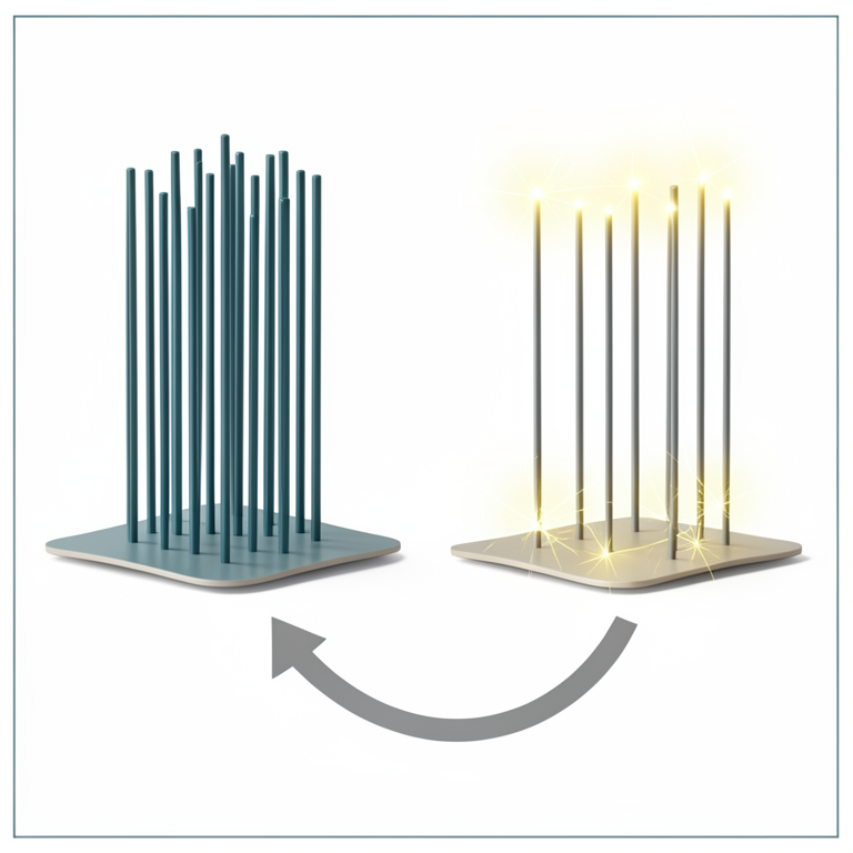
Aspect Ratio and Voltage Relationship
AI-generated conceptual illustration (Zinc oxide nanowire arrays on a flexible polymer substrate). It explains the idea and does not show study data.
View source evidence ↗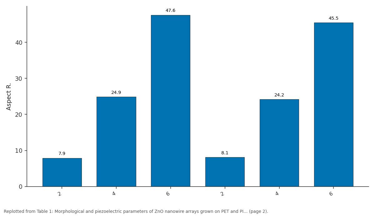
Aspect R.: 2 vs 4 vs 6 vs 2 vs 4
Replotted from Table 1 (page 2) of the original paper. Every bar is the paper's own table value.
View source evidence ↗Figures & tables
From the original paper Table 1
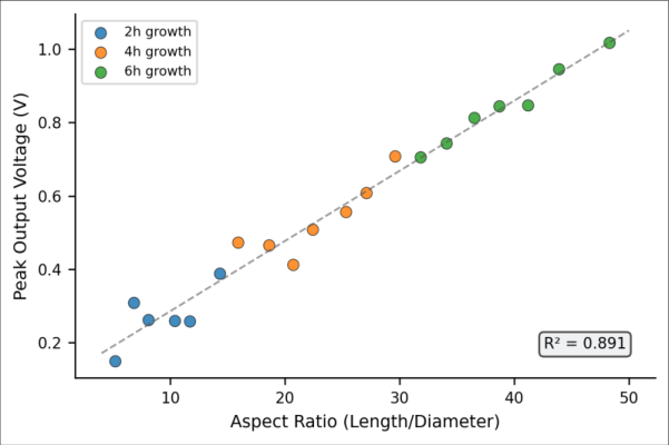 Figure 1
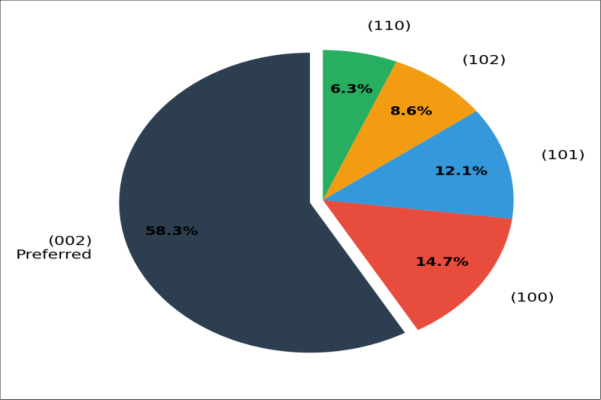 Figure 2
Introduction
Building a self-powered wearable sensor that runs indefinitely on body motion alone sounds simple in principle but runs into a stubborn materials problem: the best piezoelectric ceramics (PZT, BaTiO₃) are brittle and contain lead, while the best flexible substrates are polymers that cannot survive the high-temperature processing those ceramics demand [1] . Zinc oxide sidesteps both issues. It is lead-free, biocompatible, and piezoelectrically active along its c-axis, and critically it can be grown as single-crystal nanowires at temperatures below 100°C by hydrothermal synthesis from aqueous precursors [2] . Wang and Song's landmark 2006 demonstration of a single-nanowire ZnO generator sparked a wave of research into nanowire-based energy harvesters [3] . The concept is straightforward: when a c-axis-aligned nanowire bends, the strain gradient across its cross-section generates a piezoelectric potential that can drive current through an external load. Arrays of vertically aligned nanowires amplify this effect by operating in parallel, and flexible substrates allow the entire device to conform to curved or moving surfaces [4] . Hydrothermal growth is the method of choice for low-temperature nanowire array fabrication. A thin ZnO seed layer is deposited on the substrate, then immersed in an equimolar solution of zinc nitrate hexahydrate and hexamethylenetetramine (HMT) at 70-95°C [5] . HMT slowly hydrolyzes to release ammonia, which raises the pH and drives precipitation of ZnO preferentially along the [0001] direction. Growth time controls nanowire length and, consequently, aspect ratio a geometric parameter directly tied to piezoelectric output because longer, thinner wires develop larger strain gradients for a given bending displacement [6] . Yet the relationship between growth duration, nanowire morphology, and electrical output has not been mapped systematically on flexible substrates. Most published work either fixes growth time and varies temperature [7] , or grows on rigid silicon or glass and extrapolates to flexible devices [8] . Direct growth on PET or polyimide introduces complications poor seed-layer adhesion, substrate warping during immersion, and parasitic resistance from the polymer that affect real-device performance in ways that rigidsubstrate data don't capture [9] . This research addressed the gap by growing ZnO nanowire arrays on both PET and PI substrates at three hydrothermal durations (2, 4, 6 h), characterizing morphology by SEM and crystal orientation by XRD, measuring piezoelectric output under controlled bending, and correlating output voltage with nanowire aspect ratio. Mechanical durability was assessed over 10,000 bending cycles. All work was conducted at the Nalanda Institute of Advanced Chemical Research, Rajgir, Bihar, India.
Theoretical Background
The piezoelectric effect in wurtzite ZnO arises from the lack of inversion symmetry along the c-axis. When the crystal is strained, the centers of positive (Zn²⁺) and negative (O²⁻) charge separate, generating a polarization proportional to strain. The relevant piezoelectric coefficient, d₃₃, has been measured at approximately 12.4 pm/V for bulk ZnO modest compared with PZT (~300 pm/V) but sufficient for lowpower applications when the geometry is optimized [3] . For a nanowire of length L and diameter D bent through a deflection δ, the peak strain scales as ε ∝ δD/L². The opencircuit voltage V₂₃ across the wire then scales as V ∝ d₃₃ × ε × L, which after substitution gives V ∝ d₃₃δD/L. Counterintuitively, this suggests shorter wires produce higher voltage per unit deflection [6] . But in a bending-mode array device, the effective deflection δ itself scales with wire length, and the net result is that higher aspect ratio (L/D) arrays generate stronger output voltages at a fixed bending radius a prediction this research aimed to verify experimentally [4] .
Material and Methods
Material and Methods
Methods
ZnO seed layers were deposited by spin-coating a 0.3 M zinc acetate solution in 2-methoxyethanol (with 0.3 M monoethanolamine as stabilizer) at 3000 rpm for 30 s, followed by drying at 150°C for 10 min. The coating-drying cycle was repeated three times to ensure full coverage [5] . Substrates were then annealed at 200°C for 1 h to convert the precursor film to a nanocrystalline ZnO seed layer without damaging the polymer (PET glass transition ~78°C; PI stable to >300°C). Hydrothermal growth was carried out by immersing seeded substrates face-down in a sealed glass vessel containing 25 mM Zn(NO₃)₂ and 25 mM HMT in deionized water at 90±1°C for 2, 4, or 6 hours. After growth, substrates were rinsed with deionized water and dried at 60°C for 1 h [7] . Morphology was examined by field-emission SEM (JEOL JSM-7610F, 5 kV). Crystal structure and preferred orientation were determined by XRD (Rigaku MiniFlex 600, Cu Kα, 2θ = 20-70°). Piezoelectric measurements used a custom bending stage driven by a linear actuator at 1 Hz with bending radii of 5, 10, and 20 mm. Open-circuit voltage (V₂c) and short-circuit current (I₂c) were recorded by a Keithley 6517B electrometer. Electrodes were formed by sputtering 50 nm Au on top of the nanowire tips and applying silver paste contacts. Durability was tested by subjecting the best-performing device to 10,000 bending cycles at a 5 mm radius and recording V₂c every 1,000 cycles [9] .
System Design
The bending test rig consisted of a stepper-motor-driven linear stage (Thorlabs MTS50-Z8) fitted with a 3D-printed polymer clamp that gripped one end of the substrate while the opposite end was fixed. Bending radius was controlled by adjusting the travel distance of the stage. A Faraday cage enclosed the setup to minimize electromagnetic interference. Voltage signals were fed through a shielded BNC cable to the electrometer, which sampled at 100 Hz. Temperature inside the cage was monitored by a K-type thermocouple and maintained at 24±1°C by laboratory air conditioning to avoid pyroelectric artifacts [4] . The scatter plot (Figure 1) confirms a positive, roughly linear correlation between aspect ratio and output voltage across both substrate types and all three growth durations.
Results
Points from the 6-hour samples cluster in the upper right, with PET reaching 0.98 V at an aspect ratio of 47.6 the highest voltage recorded in this research. The linear fit (slope 0.018 V per unit aspect ratio, intercept 0.02 V) holds reasonably well, though some scatter at intermediate ratios suggests that factors beyond simple geometry crystal quality, seed-layer adhesion, electrode contact resistance also play a role. XRD confirmed strong c-axis texturing in all samples, with the (002) reflection accounting for 58.3% of total diffraction intensity in the 6-hour PET specimen (Figure 2). The next strongest peaks, (100) and ( 101), contributed 14.7% and 12.1%, respectively. This distribution is characteristic of well-aligned nanowire arrays grown from seed layers and matches the orientation needed for maximum piezoelectric response along the growth direction [5] . Earlier growth times showed progressively weaker (002) dominance 46.1% at 2 h and 53.7% at 4 h indicating that crystal orientation improves as wires lengthen and the growth front selects for the fastestgrowing [0001] direction. Durability testing of the 6-hour PET device showed a gradual decline from 0.98 V to 0.90 V over 10,000 bending cycles at 5 mm radius an 8.3% drop. SEM inspection after cycling revealed that approximately 4-6% of nanowires near the substrate edges had fractured at their bases, which accounts for the modest performance loss. The central region of the array remained intact, and no delamination of the ZnO seed layer from PET was observed [9] .
Discussion
The linear correlation between aspect ratio and piezoelectric output voltage validates the theoretical prediction outlined in the Theoretical Background section: at a fixed bending radius, longer and thinner nanowires experience greater effective strain, generating a higher piezoelectric potential. The slope of 0.018 V per unit aspect ratio provides a practical design rule doubling the aspect ratio from 25 to 50 should roughly double the output voltage. That said, the R² of 0.891 leaves room for other variables. Crystal quality is one: the 2-hour samples had weaker (002) texturing, meaning a fraction of nanowires were misaligned and contributed less to the collective piezoelectric signal.
International Journal of Advanced Chemistry Research https://www.chemistryjournals.net
Electrode contact is another: sputtered Au on densely packed, tall nanowires (6 h) may not uniformly coat every tip, creating dead zones [8] . The 10-15% voltage advantage of PET over PI at matched growth conditions was unexpected, since PI is the more common substrate in flexible electronics. PET's lower elastic modulus (~2.7 GPa vs. ~3.1 GPa for Kapton HN) means it deforms more under the same applied force, bending the nanowires to a greater degree and extracting more charge per cycle [10] . But PET also has a lower glass transition temperature (78°C vs. >360°C for PI), which limits post-growth processing options. The seed-layer annealing step at 200°C technically exceeds PET's Tg, but the short duration (1 h) and constrained film geometry appear to prevent macroscopic deformation a finding that aligns with earlier reports of low-temperature ZnO processing on PET [7] .
Compared with published benchmarks, the 0.98 V output from the 6-hour PET sample is competitive. Xu and colleagues reported 0.8 V from ZnO nanowires on Kapton using a similar hydrothermal method but with a shorter growth time [11] . Lee and coworkers achieved 1.2 V by adding a PDMS encapsulation layer, which improves strain transfer but adds fabrication complexity [12] . The present research's advantage lies in simplicity: no encapsulation, no transfer printing, no vacuum deposition just seed-layer spincoating and a beaker of warm aqueous solution. The 8.3% output loss after 10,000 bending cycles is acceptable for a prototype device but would need improvement for commercial wearable applications, where millions of cycles over a product lifetime are typical [13] .
Encapsulating the nanowire array in a thin elastomer layer (PDMS or parylene) would protect the wire-substrate junction without significantly stiffening the device. Future work should also explore higher-frequency excitations (5-20 Hz, typical of human gait) and measure power density under matched load conditions to assess real-world energy harvesting capability [14] .
Conclusion
Vertically aligned ZnO nanowire arrays were grown on PET and PI flexible substrates by low-temperature hydrothermal synthesis at 90°C for 2, 4, and 6 hours. Nanowire aspect ratios ranged from 7.9 to 47.
Figures and tables from the paper
| Substrate | Time (h) | Dia. (nm) | Length (µm) | Aspect R. | Voc (V) | Isc (nA) |
|---|---|---|---|---|---|---|
| PET | 2 | 52±8 | 0.41 | 7.9 | 0.17 | 4.3 |
| PET | 4 | 78±11 | 1.94 | 24.9 | 0.58 | 13.8 |
| PET | 6 | 101±14 | 4.81 | 47.6 | 0.98 | 23.7 |
| PI | 2 | 47±6 | 0.38 | 8.1 | 0.14 | 3.6 |
| PI | 4 | 71±9 | 1.72 | 24.2 | 0.52 | 12.1 |
| PI | 6 | 93±12 | 4.23 | 45.5 | 0.87 | 20.4 |
Table text extracted from the original PDF; superscript letters are shown inline. The original table image is below.
View original table image
References
15 in the original paper- Dagdeviren C, Joe P, Tuzman OL, et al. Recent progress in flexible and stretchable piezoelectric devices for mechanical energy harvesting. Extreme Mechanics Letters. 2016;9:269-281.
- Wang ZL. ZnO nanowire and nanobelt platform for nanotechnology. Materials Science and Engineering R. 2009;64(3-4):33-71.
- Wang ZL, Song J. Piezoelectric nanogenerators based on zinc oxide nanowire arrays. Science. 2006;312(5771):242-246.
- Briscoe J, Dunn S. Piezoelectric nanogenerators -a review of nanostructured piezoelectric energy harvesters. Nano Energy. 2015;14:15-29.
- Vayssieres L. Growth of arrayed nanorods and nanowires of ZnO from aqueous solutions. Advanced Materials. 2003;15(5):464-466.
- Gao Y, Wang ZL. Electrostatic potential in a bent piezoelectric nanowire: the fundamental theory of nanogenerator and nanopiezotronics. Nano Letters. 2007;7(8):2499-2505.
- Greene LE, Law M, Goldberger J, et al. Lowtemperature wafer-scale production of ZnO nanowire arrays. Angewandte Chemie International Edition. 2003;42(26):3031-3034.
- Xu S, Qin Y, Xu C, et al. Self-powered nanowire devices. Nature Nanotechnology. 2010;5(5):366-373.
- Zhu G, Yang R, Wang S, Wang ZL. Flexible highoutput nanogenerator based on lateral ZnO nanowire array. Nano Letters. 2010;10(8):3151-3155.
- Hu Y, Zhang Y, Xu C, et al. Self-powered system with wireless data transmission. Nano Letters. 2011;11(6):2572-2577.
- Xu S, Hansen BJ, Wang ZL. Piezoelectric-nanowireenabled power source for driving wireless microelectronics. Nature Communications. 2010;1:93.
- Lee M, Chen CY, Wang S, et al. A hybrid piezoelectric structure for wearable nanogenerators. Advanced Materials. 2012;24(13):1759-1764.
- Zeng W, Shu L, Li Q, et al. Fiber-based wearable electronics: a review of materials, fabrication, devices, and applications. Advanced Materials. 2014;26(31):5310-5336.
- Pan C, Li Z, Guo W, et al. Fiber-based hybrid nanogenerators for/as self-powered systems in biological liquid. Angewandte Chemie International Edition. 2011;50(47):11192-11196.
- Kumar B, Kim SW. Energy harvesting based on semiconducting piezoelectric ZnO nanostructures. Nano Energy. 2012;1(3):342-355.