
Research article · 2018 · Full text
International Journal of Statistics and Applied MathematicsHigh arrangement group quantum circuits Hilbert spaces for in sequence special consideration
Volume 3(3) · Pages 51–60
Research areasQuantum Computing Algorithms and ArchitectureOptical Network TechnologiesNeural Networks and Reservoir Computing
Abstract
Author-writtenA quantum circuit is a model for Hilbert space computation in which a computation is a sequence of quantum spaces, which are reversible transformations on a quantum mechanical space of an n-bit register. This analogous structure is referred to as an n-space register. We define and can build efficient depth-universal and almost size-universal quantum circuits Such circuits can be viewed as general purpose simulators for central classes of quantum circuits and can be used to capture the computational power of the circuit class being simulated. For depth we construct universal circuits whose depth is the same order as the circuits being simulated. For size, there is a log factor blow-up in the universal circuits constructed here. The architecture scalability afforded by recent proposals of a large-scale photonic-based quantum space computer allows us to move on to a discussion of High performance Hilbert quantum circuits.
Summary
Source-checkedPlain-language reading of the full paper, prepared with AI and checked against the text. Each point links to the authors' own words.
Why it matters
- Quantum circuits serve as models for Hilbert space computation, utilizing reversible transformations on an n-bit register. View evidence ↗
- Studying universal circuits for quantum circuit classes helps researchers understand the computational strength and limitations of those circuits. View evidence ↗
- More efficient constructions of universal circuits lead to smaller physical processors for the corresponding circuit class. View evidence ↗
The question
- The authors aim to construct a single family of quantum circuits that can efficiently simulate all circuits within a natural class C. View evidence ↗
What they did
- The study examines depth-universal circuits using gate families F (Hadamard, π/8, and fan-out gates) and F' (which adds Toffoli gates). View evidence ↗
- The authors utilize Z gates and Z-fanout gates to run all possible gates for a layer in parallel, as these gates only modify the phase. View evidence ↗
- To construct size-universal circuits for fanin-2 circuits, the authors apply Valiant's concept of universal graphs. View evidence ↗
What they found
- Depth-universal quantum circuits exist for gate families F and F', requiring O(n2d) qubits and allowing for log-space uniform construction. View evidence ↗
- The authors found a family of universal circuits that can simulate any circuit with c gates on n qubits with a size of k(n + c) log(n + c). View evidence ↗
- For circuits consisting of Hadamard, π/8, and unbounded Toffoli gates, a universal circuit family exists with a size of O(nc log(nc)). View evidence ↗
What it means
- The authors conclude that 3D topological clusters in optics enable conceptual scaling for large mainframes beyond the capabilities of other quantum information processing architectures. View evidence ↗
- The authors state that partitioning resources for an optimal multi-user device remains a complicated networking problem. View evidence ↗
- The authors note they do not know how to universally simulate depth-d circuits over {H, T, CNOT} in depth O(d) without the use of fan-out gates. View evidence ↗
Visual summary
1 visualsIllustrations explain the paper; they do not show study data.
Universal Quantum Circuit Concept
AI-generated conceptual illustration (Quantum circuit hardware components). It explains the idea and does not show study data.
View source evidence ↗Figures & tables
From the original paper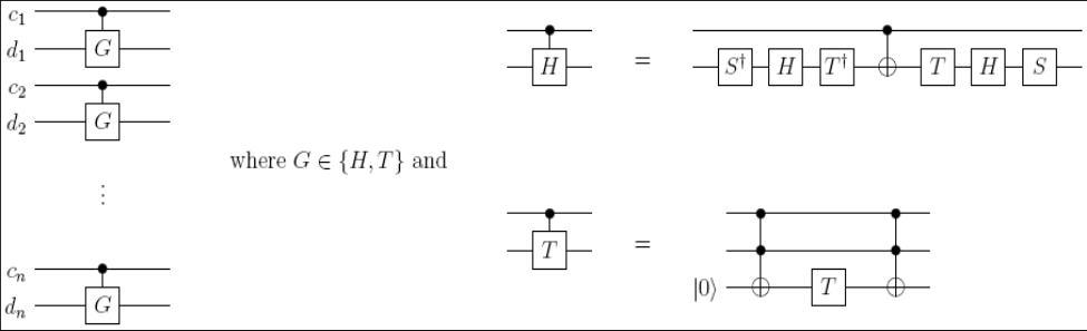 Figure 1
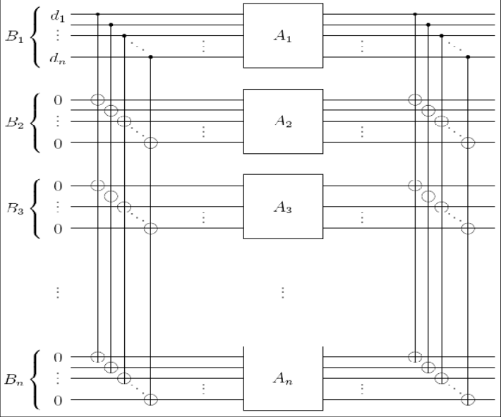 Figure 2
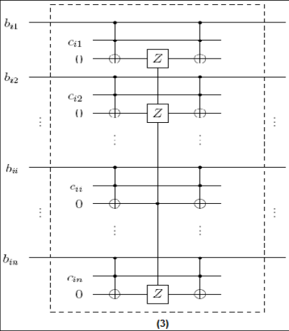 Figure 3
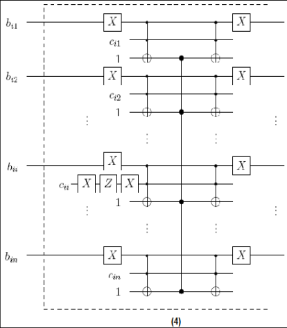 Figure 4
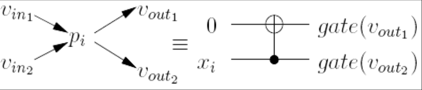 Figure 5
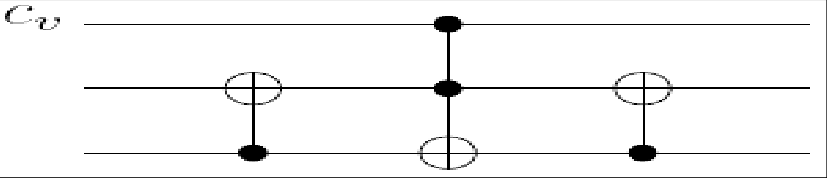 Figure 6
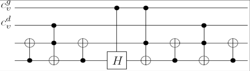 Figure 7
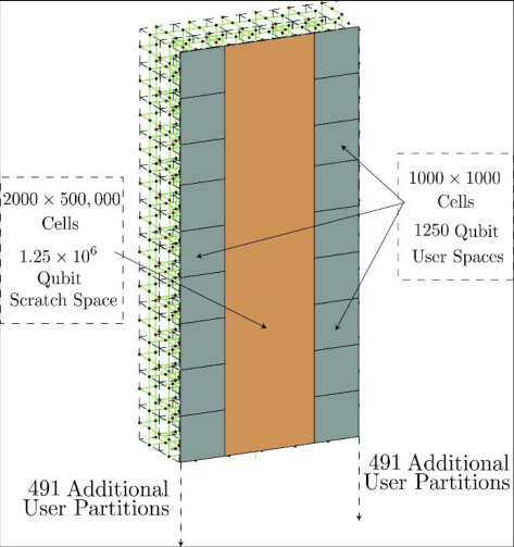 Figure 8
Introduction
A number of necessary ideas that form the basis for the study of quantum computation are briefly reviewed here.
1.1 Linear Superposition: Linear superposition is closely related to the familiar mathematical principle of linear combination of vectors. Quantum systems are described by a wave function that exists in a Hilbert space. The Hilbert space has a set of states, | i that form a basis, and the system is described by a quantum state
is said to be coherent or to be in a linear superposition of the basis states| i , and in general the coefficients c i are complex. A postulate of quantum mechanics is that if a coherent system interacts in any way with its environment (by being measured, for example), the superposition is destroyed. This loss of coherence is governed by the wave function. The coefficients c i are called probability amplitudes, and |ci| 2 gives the probability of | being measured in the state| i . Note that the wave function describes a real physical system that must collapse to exactly one basis state. Therefore, the probabilities governed by the amplitudes ci must sum to unity. A two-state quantum system is used as the basic unit of quantum computation. Such a system is referred to as a quantum bit or qubit and naming the two states |0 and |1.
Interference:
Interference is a familiar wave phenomenon. Wave peaks that are in phase interfere constructively while those that are out of phase interfere destructively. This is a phenomenon common to all kinds of wave mechanics from water waves to optics. The wellknown double slit experiment demonstrates empirically that at the quantum level interference also applies to the probability waves of quantum mechanics. The wave function interferes with itself through the action of an operator-the different parts of the wave function interfere constructively or destructively according to their relative phases just like any other kind of wave.
Entanglement:
Entanglement is the potential for quantum systems to exhibit correlations that cannot be accounted for classically. From a computational standpoint, entanglement seems intuitive enough-it is simply the fact that correlations can exist between different qubits-for example if one qubit is in the |1 state, another will be in the |1 state. However, from a physical standpoint, entanglement is little understood. The questions of what exactly it is and how it works are still not resolved. What makes it so powerful (and so little understood) is the fact that since quantum states exists as superposition's, these correlations exist in superposition as well. When coherence is lost, the proper correlation is somehow communicated between the qubits, and it is this "communication" that is the crux of entanglement. Mathematically, entanglement may be described using the density matrix formalism. For example, the quantum state
Quantum input and output:
states -There is no way to efficiently prepare the input state ψ for a quantum circuit. This does not prevent quantum circuits for the discrete Fourier transform from being used as intermediate steps in other quantum circuits, but the use is more subtle. In fact quantum computations are probabilistic. We are using a mathematical model for how quantum circuits can simulate probabilistic but classical computations. Consider an r-qubit circuit U with register space H QB(r) . U is thus a unitary map In order to associate this circuit to a classical mapping on bit strings or information, we specify An input register X = {0, 1} m of m (classical) bits of information. An output register Y = {0, 1} n of n (classical) bits of information.
introduction to universal quantum circuit:
Like resource-bounded universal Turing machines, efficiently constructed universal circuits capture the hardness of languages computed by circuits in a given circuit class. As a result, the study of the existence and complexity of universal circuits for quantum circuit classes provides insight into the computational strength of such circuits, as well as their limits. There is both a theoretical and a practical aspect to this study. The existence of a universal circuit family for a complexity class defined by resource bounds (depth, size, gate width, etc.) provides an upper bound on the resources needed to compute any circuit in that class. It also opens up possibilities for proving lower bounds on the hard languages in the class; as such bounds would follow from a lower bound proof for the language computed by a universal circuit family for the circuit class. More precisely, the specific, efficient construction of a universal circuit for a class of circuits yields, for a fixed input size, a single circuit which can be used to carry out the computation of every circuit (with that same input size) in that family, basically a chip or processor for that class of circuits. The more efficient the construction of the universal circuit, the smaller the processor for that class. Furthermore, the universal circuit is in a sense a compiler for all possible computations of all circuits in this family. It can be used to efficiently program all possible computations capable of being carried out by circuits in this type of circuits, and in doing so inevitably acts as a general purpose simulator and with as little loss of efficiency as is possible. In the case of quantum circuits there are specific issues relating to the necessities that computations must be clean and reversible which come into existence, and to an extent complicate the classical methods. Our motivation for this work instigates with classical results due to Cook, Valiant, and others [1,18] . Cook and Hoover considered depth universality and described a depth-universal uniform circuit family for circuits of depth Ω (log n). Valiant studied size universality and disclosed how to construct universal circuits of size O (s log s) to simulate any circuit of size s.
Definition 1: (Universal Quantum Circuits).
Fix n > 0 and let C be a collection of quantum circuits on n qubits. A quantum circuit U on n + m qubits is universal for C if, for every circuit C ∈ C, there is a string x ∈ {0, 1} m (the encoding ) such that for all strings y ∈ {0, 1} n (the data),
The circuit collections we are interested in are usually defined by bounding various parameters such as the size (number of gates), depth (number of layers of gates acting simultaneously on disjoint sets of qubits), or palette of allowed gates (e.g. Hadamard, π/8, CNOT). As in the classical case, we also want our universal circuits to be efficient in various ways. For one, we restrict them to using the same gate family as the circuits they simulate. We may also want to restrict their size or the number m of qubits they use for the encoding. We are particularly concerned with the depth of universal circuits.
Theorem 3. Depth-universal quantum circuits exist over F and over F′. Such circuits use O (n 2 d) qubits and can be built logspace uniformly in n and d.
Note that the results for the two circuit families are independent, because it is not known whether n-qubit Toffoli gates can be implemented exactly in constant depth using single-qubit gates and fan-out gates, although they can be approximated this way [3].
It would be nice to find depth-universal circuits over families of bounded-width gates (no. of qubits) such as {H, T, CNOT}. Depth-universal circuits with bounded-width gates, if they exist, must have depth Ω (logn) and thus can only depth efficiently simulate circuits with depth Ω (log n). This can be easily seen as follows: Suppose all you wanted was a universal circuit U for depth-1 circuits on n-qubits that use CNOT gates only. Since any pair of the n qubits could potentially be connected with a CNOT gate, that pair must be connected somehow (indirectly perhaps) within the circuit U. Thus any data input qubit can potentially affect any of the other n-1 data output qubits. Since U only has constant-width gates, the number of qubits affected by any given data input increases by only a constant factor per layer, and so U must have Ω (log n) layers.
One can therefore only hope to find depth-universal circuits for circuits of depth Ω (log n) over bounded-width gates. Although such circuits exist in the classical case (see below), we are unable to construct them in the quantum case (see Section 7).
Other significant work
Most of the research on universal quantum circuit classes concords with finding small, natural, universal sets of gates which can be used in quantum circuits to efficiently simulate any quantum computation. Our problem and point of view here is quite different. We have the goal of constructing, for a natural class C of quantum circuits, a single family of quantum circuits which can efficiently simulate all circuits on the class C. In this paper we consider classes C which have significant resource bounds (small or even constant depth, or fixed size) and ask that the corresponding universal circuits family to have similar depth or size bounds.
Cook and Hoover [1] considered the problem of constructing general purpose classical (Boolean) circuits using gates with fan-in two. They asked whether, given n, c, d, there is a circuit U of size c O (1) and depth O(d) that can simulate any n-input circuit of size c and depth d. Cook and Hoover constructed a depth-universal circuit for depth Ω(log n) and polynomial size, but which takes as input a custom-built encoding of the circuit, and they also presented a circuit with depth O(log n log log n) to convert the standard encoding of the circuit to the required encoding.
Valiant looked at a similar problem-trying to minimize the size of the universal circuit [6] . He considered classical circuits built from fan-in 2 gates (but with unbounded fan-out) and embedded the circuit in a larger universal graph. Using switches at key vertices of the universal graph, any graph (circuit) can be embedded in it. He managed to create universal graphs for different types of circuits and showed how to construct a O(c log c)-size and O(c)-depth universal circuit. He also showed that his constructions have size within a constant multiplicative factor of the information theoretic lower bound. For quantum circuits, Nielsen and Chuang (in [4] ) considered the problem of building generic universal circuits, or programmable universal gate arrays as they call them. Their universal circuits work on two quantum registers, a data register and a program register. They do not consider any size or depth bound on the circuits and show that simulating every possible unitary operation requires completely orthogonal programs in the program register. Since there are infinitely many possible unitary operations, any universal circuit would require an infinite number of qubits in the program register. This shows that it is not possible to have a generic universal circuit which works for all circuits of a certain input length. However they showed that it is possible to construct an extremely weak type of probabilistic universal circuit with size linear in the number of inputs to the simulated circuit. Sousa and Ramos considered a similar problem of creating a universal quantum circuit to simulate any quantum gate [7] . They construct a basic building block which can be used to implement any single-qubit or CNOT gate on n qubits by switching certain gates on and off. They revealed how to combine several of these building blocks to implement any n-qubit quantum gate for information processing.
Outline of the paper
For the rest of the paper, we will use HPQC to denote high performance quantum computer, U to denote the universal circuit and C to denote the circuit being simulated. We define the quantum gates we will use in Section 2. The construction of depth-universal circuits is in Section 3. We briefly describe the construction of almost-size-universal quantum circuits in Section 4. We described the high performance quantum circuits for information processing in section 5. We mention a couple of miscellaneous results in Section 6.
Inceptions
We assume the standard notions of quantum states, quantum circuits, and quantum gates described in [5], in particular, H (Hadamard), T (π/8), S = T 2 (phase), and CNOT (controlled NOT). We will also need some additional gates, which we now motivate. The depth-universal circuits we construct require the ability to feed the output of a single gate to many other gates. While this operation, commonly known as fan-out, is common in classical circuits, copying an arbitrary quantum state unitarily is not possible in quantum circuits due to the no-cloning theorem [5]. It turns out that we can construct our circuits using a classical notion of fan-out operation, defined as the fan-out gate for any of the standard basis states |c (the control) and |t 1 ,..., |t n (the targets) and extended linearly to other states 5 [2] . F n can be constructed in depth log n using CNOT gates. We need to use unbounded fan-out gates to achieve full depth universality. We also use the unbounded Toffoli gate g∧ n (X):
We reserve the term "Toffoli gate" to refer to the (standard) Toffoli gate ∧ 2 (X), which is defined on three qubits. In addition to the fan-out gate, our construction requires us to use controlled versions of the gates used in the simulated circuit. For most of the commonly used basis sets of gates (e.g., Toffoli gate, Hadamard gate, and phase gate S), the gates themselves are sufficient to construct their controlled versions (e.g., a controlled Hadamard gate can be constructed using a Toffoli gate and Hadamard and phase gates). Depth or size universality requires that the controlled versions of the gates should be constructible using the gates themselves within proper depth or size, as required.
Definition 4 (Closed under controlled operation).
A set of quantum gates G = {G1...} is said to be closed under controlled operation if for each G i 2 G, the controlled version of the gate
can be implemented in constant depth and size using the gates in G. Here, |c is a single qubit and G i could be a single or a multi-qubit gate.
Note that CNOT = F 1 , and given H, T, and CNOT we can implement the Toffoli gate via a standard constant-size circuit [5] . We can implement the phase gate S as T 2 , and since T 8 = I, we can implement S † = T 6 and T † = T 7 . A generalized Z gate, which we will hereafter refer to simply as a Z gate, is an extension of the single-qubit Pauli Z gate (|x (-1) x |x) to multiple qubits:
A Z gate can be constructed easily (in constant depth and size) from a single unbounded Toffoli gate (and vice versa) by conjugating the target qubit of the unbounded Toffoli gate with H gates (i.e., placing H on both sides of the Toffoli gate on its target qubit).Similarly, a Z-fanout gate Z n applies the single-qubit Z gate to each of n target qubits if the control qubit is set:
A Z n gate can be constructed from a single Fn gate and vice versa in constant depth (although not constant size) by conjugating each target with H gates. So, in our depth-universal circuit construction, we can use these either or both of these types of gates. Similarly for unbounded Toffoli versus Z gates. Z gatesand Z-fanout gates are important because they only change the phase, leaving the values of the qubits intact (they are represented by diagonal matrices in the computational basis). This allows us to use a trick due to Høyer and Spalek [3] and run all possible gates for a layer in parallel.
Depth-universal quantum circuits
In this section, we prove Theorem 3, i.e. that depth-universal circuits exist for each of the gate families
We first give the proof for F then show how to modify it for F ′. The depth-universal circuit U we construct simulates the input circuit C layer by layer, where a layer consists of the collection of all its gates at a fixed depth. C is encoded in a slightly altered form, however. First, all the fanout gates in C are replaced with Zfanout gates on the same qubits with H gates conjugating the targets. At worst, this may roughly double the depth of C (adjacent H gates cancel). Each layer of the resulting circuit is then separated into three adjacent layers: the first having only the H gates of the original layer, the second only the T gates, and the third only the Z-fanout gates. U then simulates each layer of the modified C by a constant number of its own layers. We describe next how these layers are constructed.
Simulating single-qubit gates.
The circuit to simulate an n-qubit layer of single qubit gates of type G, say, consists of a layer of controlled-G gates where the control qubits are fed from the encoding and the target qubits are the data qubits. Figure 1 shows a layer of G gates, where G {H, T}, controlled using H, S, T, CNOT, and Toffoli gates. To simulate G gates on qubits
To simulate some Z-fanout gate G of C whose control is on the ith qubit, say, we do this in block Bi by setting c ii to 1 and setting c ij to 1 for every j where the j th qubit is a target of G. All the other c-qubits in B i are set to 0. We can do this in separate blocks for multiple Z-fanout gates on the same layer, because no two gates can share the same control qubit. Any c-qubits in unused blocks are set to 0. Simulating unbounded Toffoli gates. We can modify the construction above to accommodate unbounded Toffoli gates (gate family F ′), or equivalently Z gates, by breaking each layer of C into four adjacent layers, the first three being as before, and the fourth containing only Z gates. The top-level circuit to simulate a layer of Z gates looks just as before (Figure 2), except now each A i subcircuit looks a bit different and is shown in Figure 4, where the central gate is a Z gate connecting the ancillae.
As before, the qubits c i1 ... c in are encoding qubits. The XZX gates on c ii multiply the overall phase by
To simulate some Z gate G of C whose first qubit is i, say, we do this in block B i by setting c ii to 1 and setting c ij to 1 for every j where the jth qubit is part of G. All the other c-qubits in B i are set to 0. As before, we can do this in separate blocks for multiple gates on the same layer, because no two gates can share the same first qubit. Any c-qubits in unused blocks are set to 0, and it is easy to check that this makes the block have no net effect.
Size-universal quantum circuits spaces
Similar to a depth-universal circuit, a size-universal circuit is a universal circuit with the same order of the number of gates as the circuit it is simulating. Formally, Definition 5. A family {U n,c } of universal circuits for n-qubit circuits of size c is size-universal if SIZE (U n,c ) = O(c). A simple counting argument shows that it is not possible to obtain a completely size-universal circuit for fanin-2 circuits. Consider all circuits with c fanin-2 gates where one input of each gate is the first qubit. There are (n-1)c possible circuits. Then consider similar circuits where there is no gate with input as the first qubit and continue recursively. Thus the number of possible fanin-2 circuits is (n-1) c . Since all the encoding bits have to be connected to some of the fanin-2 gates in the universal circuit, it must have (c log n) gates. We use Valiant's idea of universal graphs [6] to construct a universal family of fanin-2 circuits that are very close to the aforementioned lower bound. As before, we would like to simulate C by using the same set of gates used in C. Our construction works for any circuit using unbounded Toffoli gates and any set of single-qubit and 2-qubit gates closed under the controlled operation. First we will define a universal directed acyclic graph with n special vertices (called poles) in which we can embed any circuit with n gates (considering the inputs also as gates). The embedding will map the wires in the circuit to paths in the graph. Definition 6 (Edge-embedding [6] ). An edge-embedding of G = (V, E) into G′ = (V′,E′) maps V one-to-one to V′ and maps each edge (i, j) E to a directed path (i) (j) in G′ such that distinct edges are mapped to edge disjoint paths. The graph of any circuit of size n can be represented as a directed acyclic graph with vertices {1,...,,n} such that there is no edge from j to i for i < j and each vertex has fanin and fanout 2. Let 2 (n) be the set of all such graphs. Definition 7 (Edge-universal graph [6] ). A graph G′ is edge-universal for 2 (n) if it has distinct poles p 1 ,..., p n such that any graph G 2 (n) can be edge-embedded into G′ where each vertex i G is mapped to vertex (i) = p i G′. Then, Valiant shows how to construct a universal graph.
Theorem 8 ( [6] ).
There is a constant k such that or all n there exists an acyclic graph G′ that is edge-universal for 2 (n), and G′ has kn lg n vertices,each vertex having fanin and fanout 2. It is fairly easy to construct a universal circuit using the universal graph. In fact, the universal circuit for circuits with n inputs and c gates will be any edge-universal graph for 2 (n + c). Consider any such edge-universal graph G′. Then G′ has c′ = k (n+c) log (n+c) vertices for some k. These c′ vertices include fixed poles p 1 ... p n , p n+1 ... p n+c and non-pole vertices. Create a quantum circuit C′ with c′ gates (including the inputs and outputs) where G′ describes how the gates connect to each other. For each of the vertices p 1 ... p n of G′, remove their incoming edges and replace the vertices by the input as shown in Figure 5. Replace each of the vertices p n+1 ... p n+c with a sub-circuit that applies any of the single-or 2-qubit gates on the inputs, where the gate to apply is controlled by the encoding. E.g. Figure 7 shows the gates at a pole vertex in a universal circuit simulating CNOT and H gates. For a non-pole vertex, replace it with a subcircuit that swaps the incoming and outgoing wires (i.e. first input is connected to second output and second input is connected to first output) or directly connects them (i.e. first input is connected to first output and similarly for the second input). Again, the subcircuit is controlled by the encoding which controls whether to swap or directly connect (see Figure 6). The edge disjointness property guarantees that wires in the embedded circuit are mapped to paths in C0 which can share a vertex but cannot share any edge. C specify which qubit the gate acts on (for H gate) or which is the control qubit (for CNOT gate).
To simulate any fanin-2 circuit C with c gates acting on n qubits, construct the edge-universal graph G′ for 2 (n + c). Embed the graph of C into G′ such that the input nodes of Care mapped to the poles p 1 ... p n in G′. Now for each gate of the circuit, consider the pole to which it was mapped. Set a bit in the encoding to denote the type of the gate at that pole. For the non-pole vertices, set a bit in the encoding to specify whether the two input values should be swapped or mapped directly to the two output values. The size of the encoding is (n+c) (log |gates|+1) + (| 2 (n+c) |-(n+c)) which is O(c log c) for polynomial size circuits. This construction gives us a universal circuit with a logarithmic blow-up in size.
Theorem 9.
There is a constant k and a family of universal circuits U n,c that can simulate every circuit with c gates acting on n qubits such that SIZE(U n,c ) = k(n + c) log(n + c). We can use a similar idea for circuits with unbounded fanin. First we decompose the unbounded fanin gates using bounded fanin gates (fanin 2 in this case). This is doable for most of the common unbounded fanin gates. For example, an unbounded Toffoli gate of size f can be constructed using (f) successive Toffoli gates of size 3, which can in turn be implemented using Hadamard, phase, /8 and CNOT gates [5]. So any circuit of size c consisting of Hadamard, /8 and unbounded Toffoli gates can be transformed into an equivalent circuit with size at most O (cn) consisting of these single-qubit gates and CNOT gates. The rest of the construction follows as before.
Corollary 1.
There is a family of universal circuits U n,c that can simulate quantum circuits of size c on n qubits and consisting of Hadamard,/8, and unbounded Toffoli gates such that SIZE(U n,c ) = O(nc log(nc)).
High performance universal quantum circuit
The issue of computational scalability for QIP (quantum information processing) circuit has been an intensive area of research for not only physicists but also computer scientists, mathematicians and network analysts and in the past decade have been many proposals for scalable quantum devices for a variety of quantum architectures [8][9][10][11][12][13][14][15][16] . The complexity in designing a large scale quantum computer is immense and research in this area must incorporate complex ideas in theory, quantum error correction, quantum algorithms and network design. Due to the relative infancy of theoretical and experimental QIP it has been difficult to implement theoretically scalable ideas in quantum information theory, error correction and algorithm design into an architectural model where the transition from 1-100qubits to 1-100 million qubits is conceptually straight forward. Recent theoretical advancements in computational models for QIP has introduced an extremely elegant pathway to realize an enormously large QIP circuit induced by Raussendorf, Harrington and Goyal [17][18][19] has emerged as an extremely promising computational model for QIP. Integration of this model with chip-based photon/photon gates such as the photonic module [13] has lead to a promising optical realization of a quantum computer. The conceptual scalability of the chip based topological computer allows, for the first time, a grounded discussion on large scale quantum information processing, beyond the individual computer. The 3-dimensional cluster lattice can be developed as a generic resource for high performance quantum information processing (HPQIP). The architectural model of 3D topological clusters in optics allows for the conceptual scaling of a large topological cluster mainframe well beyond what could theoretically be done with other architectures for QIP.
Other results
Other results
Circuit encoding:
We have been mostly concerned with the actual simulation of a quantum circuit C by the universal circuit U. It is possible, however, to hide some complexity of the simulation in U's description of C itself. Usually, the description of a classical circuit describes the underlying graph of the circuit and specifies the gates at each vertex. We can similarly describe a quantum circuit by its graph structure. The description is extremely compact with size proportional to the size of the circuit. However, we use a description that is more natural for quantum circuits and especially suitable for simulation. The description stores the grid structure of the circuit; the rows of the grid correspond to the qubits, and the columns correspond to the different layers of the circuit. This description is not unique for any given circuit and its size is O(nd), where n is the number of qubits (information) and d is the depth of the circuit. A graph-based description can be easily converted to this grid-based description in polynomial time.
Limitations and open problems
Although the preparation of a large 3D cluster lattice with photonic chips has been developed, how to partition resources for an optimal, multi-user device is a complicated networking problem. At this stage we will simply present an example partition structure for the resource lattice, hopefully demonstrating some of the essential features that would be needed for this model. We will approach this analysis with some basic numerical estimates to give an idea of the resource costs and physical lattice sizes for a mainframe device. An HPQC mainframe will consists of two regions, outer region corresponding to user partitions and an inner region which we will denote as scratch space. A number of natural, interesting open problems remain in the case of universal circuits. Fan-out gates are used in our construction of a depth-universal circuit family. Is the fan out gate necessary in our construction? We believe it is. In fact, we do not know how to simulate depth-d circuits over {H, T, CNOT} universally in depth O (d) without using fan-out gates, even assuming that the circuits being simulated have depth (log n). The shallowest universal circuits with bounded width gates we know of have a lg n blow-up factor in the depth, just by replacing the fanout gates with logdepth circuits of CNOT gates.
Our results apply to circuits with very specific gate sets. How much can these gate sets are generalized? Are similar results possible for any countable set of gates containing Hadamard, unbounded Toffoli, and fan-out gates?
We showed how to construct a universal circuit with a logarithmic blow-up in size. The construction is within a constant factor of the minimum possible size for polynomial-size, bounded-fan-in circuits. However for constant-size circuits, we believe the lower bound can be tightened to match the proven upper bound. For unbounded-fan-in circuits, we construct a universal circuit with size O (nc log nc) which is significantly larger than the bounded fan-in lower bound of (c log n).
We think that a better lower bound is possible for the unbounded-fan-in case.
Figures and tables from the paper
References
26 in the original paper- Stephen A, Cook and H. James Hoover. A depth-universal circuit. SIAM Journal of Computing. 1985; 14(4):833-839.
- Fang M, Fenner S, Green F, Homer S, Zhang Y. Quantum lower bounds for fanout. Quantum information and Computation. 2006; 6(1):046-057.
- Høyer P, Spalek R. Quantum circuits with unbounded fan-out. Theory of Computing. 2005; 1:81-103.
- Nielsen MA, Chuang IL. Programmable quantum gate arrays. darxiv: quant-ph/9703032v1, 1997.
- Nielsen MA, Chuang IL. Quantum Computation and Quantum Information. Cambridge University Press, 2000.
- Leslie G. Valiant. Universal circuits (preliminary report). In Proceedings of the 8th ACM Symposium on the Theory of Computing, [Yao] A. CC. Yao. Quantum circuit complexity. In Proceedings of the 34 th IEEE Symposium on Foundations of Computer Science, 1976, 1993, 196-203, 352-361.
- Sousa PBM, Ramos RV. Universal quantum circuit for n-qubit quantum gate: A programmable quantum gate. Quamtum Information and Computation. 2007; 7(3):228-242.
- Kielpinski D, Monroe C, Wineland DJ. Architecture for a large-scale ion-trap quantum computer, Nature. 2002; 417:709-711.
- Taylor JM. Fault-tolerant architecture for quantum computation using electrically controlled semiconductor spins, Nature Phys. 2005; 1:177-183.
- Hollenberg LCL, Greentree AD, Fowler AG, Wellard CJ. Two-dimensional architectures for donor-based quantum computing, Phys. Rev. B. 2006; 74:045311.
- Fowler AG. Long-range coupling and scalable architecture for superconducting flux qubits, Phys. Rev. B. 2007; 76:174507.
- Devitt SJ. Architectural design for a topological cluster state quantum computer, New. J Phys. 2009; 11:083032.
- Stock R, James DFV. Scalable, High Speed Measurement-Based Quantum Computer Using Trapped Ions, Phys. Rev. Lett. 2009; 102:170501.
- Mamoto. Distributed Quantum Computer Architecture Using Semiconductor Nanophotonics, Int. J Quant. Info. 2010; 8:295323.
- Herrera-Marti DA, Fowler AG, Jennings D, Rudolph T. Photonic implementation for the topological cluster-state quantum computer, Phys. Rev. A. 2010; 82:032332.
- Cody Jones N. A Layered Architecture for Quantum Computing Using Quantum Dots, ar Xiv: 1010.5022, 2010.
- Raussendorf R, Harrington J. Fault-Tolerant Quantum Computation with High Threshold in Two Dimensions, Phys. Rev. Lett. 2007; 98:190504.
- Raussendorf R, Harrington J, Goyal K. Topological fault-tolerance in cluster state quantum computation, New J Phys. 2007; 9:199.
- Fowler AG, Goyal K. Topological cluster state quantum computing, Quant. Inf. Comp. 2009; 9(9 & 10):721-738.
- Devitt SJ. Photonic module: An on-demand resource for photonic entanglement, Phys. Rev. A. 2007; 76:052312.
- Raussendorf R, Briegel HJ. A One-Way Quantum Computer, Phys. Rev. Lett. 2001; 86:5188.
- Villoresi P. Experimental verification of the feasibility of a quantum channel between space and Earth, New. J Phys. 2008; 10:033038.
- Ursin R. Proc. Microgravity Sciences and Process Symposium SECOQC, 2008. Project www.sqcoqc.net.
- Munro WJ. From quantum multiplexing to high-performance quantum networking, Nature Photonics. 2010; 4:792-796.
- Bravyi S, Kitaev A. Universal quantum computation with ideal Clifford gates and noisy ancillas, Phys. Rev. A. High performance quantum computing. 2005; 71:022316.
- Fowler AG. Towards Large-Scale Quantum Computation, quant-ph/0506126, 2005.